



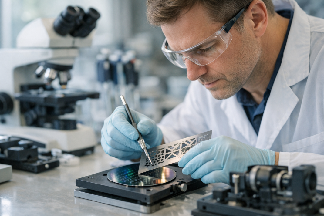
New stencil method developed by Skoltech together with teams from Harbin Institute of Technology and ITMO University demonstrates a way to deposit complex geometric arrangements of carbon nanotubes in a single stage while minimizing material loss. The technique uses reusable stencils to guide the placement of nanotube material, allowing intricate patterns to be transferred without the multi-step lithography or mask disposal that often accompanies standard microfabrication workflows.
The patterned networks produced with this approach are tailored for applications in advanced optical components and in mechanical strain sensing for monitoring structural integrity. Precise arrangements of nanotubes can determine optical response, electrical pathways and mechanical sensitivity, making pattern fidelity critical for device performance. By reducing discarded material and avoiding one-time consumables, the method addresses a persistent efficiency challenge in the handling of nanomaterials used in photonics and sensor technology. Related research fields include nanotecnologia and sensori, where the balance between precision and resource use is central to scaling lab demonstrations into manufacturable products.
Technically, the advantage stems from combining pattern definition and material deposition into a consolidated operation: a stencil physically defines the geometry while serving as a reusable transfer medium. This reduces process steps and the need for sacrificial masks or etching sequences, simplifying production workflows. The stencil-based deposition can accommodate elaborate geometries that are difficult to achieve with blanket coating methods followed by subtractive patterning, and it limits exposure of nanotube material to wasteful handling stages.
The collaborative work underlines a pathway toward more sustainable fabrication of nanoscale components used in photonics, flexible electronics and structural sensors. If adopted beyond proof-of-concept demonstrations, the approach could make certain device classes less resource-intensive to produce and easier to prototype. Continued work will determine compatibility with different substrates and integration into existing manufacturing lines, while the interdisciplinary partnership highlights ongoing international momentum in applied nanomaterials research.